
AP03B STM32 MCU
Documentation: Design reference available; AP03B upload instructions in preparation
Explore with your favorite AI
 ChatGPT
  Claude
 Gemini & other AI
Copy this page’s context into your AI to explore how it works and what you can build.
 Open Gemini
 Copy the prompt, then paste it into Gemini’s message box.
View prompt
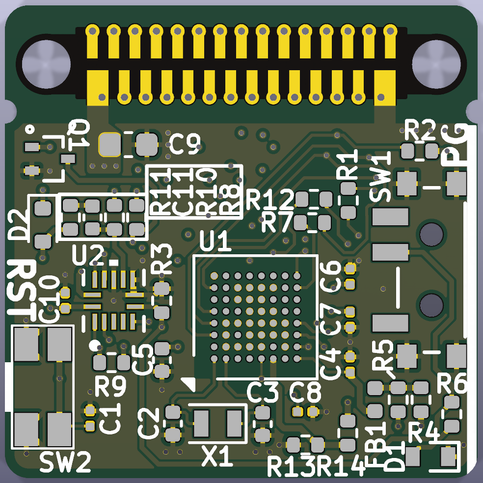
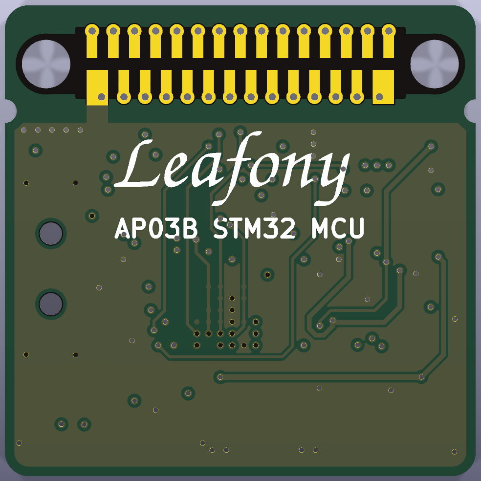
These reference images were generated from the KiCad board data. Component 3D models are omitted, and pads for unpopulated components are included.
Features
Section titled “Features”This MCU (microcontroller) leaf runs programs to read sensors and control communication leaves and other modules. It is a redesigned version of AP03 STM32 MCU, using the STMicroelectronics STM32L452REI6.
It connects to other leaves through the Leafony Bus and operates from 3.3V. The board includes a PG switch for BOOT0, a reset switch, and an LED indicating the BOOT0 state. It is the MCU leaf in the Cellular LPWA Cat-M1 Kit.
Specifications
Section titled “Specifications”| Item | Description |
|---|---|
| MCU | STMicroelectronics STM32L452REI6 |
| CPU | Arm Cortex-M4 with FPU |
| Maximum clock | 80 MHz (MCU specification) |
| Flash memory | 512 KB |
| SRAM | 160 KB |
| Power | Leafony Bus 3.3V / GND |
| Low-speed external clock | 32.768 kHz crystal (X1) |
| Main bus signals | D0–D13, A0–A5, SDA / SCL, SWDIO / SWCLK, RESET |
| Bus contacts | 29 contacts on each side (CN1) |
| Board dimensions | 20 × 20 mm (PCB design dimensions) |
| Board thickness / layers | 0.8 mm, 6 layers (excluding component height) |
| Design revision | v1.0, April 27, 2026 |
See STMicroelectronics product information for CPU and memory specifications. The actual clock depends on the firmware configuration.
Power and external connections
Section titled “Power and external connections”Supply the Leafony Bus 3.3V terminal from a power leaf or other suitable source. The VBUS terminal is not connected to the AP03B circuitry. There is no USB connector on the board; provide a separate interface for a computer or debugger.
SDA and SCL each have a 10 kΩ pull-up resistor to 3.3V. Before connecting external devices, check the Leafony Bus specification and the other device’s power and signal voltages.
AREF connection resistor R5 is DNP (not populated), so the bus AREF terminal is not connected to the MCU’s analog supply/reference circuit in the standard configuration.
Pin connections
Section titled “Pin connections”The following table describes the standard Leafony Bus to MCU connections. Front and back contacts with the same number (such as F1 / B1) carry the same signal. MCU port names are schematic names, not Arduino sketch pin numbers.
| Contact (front / back) | Leafony Bus signal | MCU port / connection |
|---|---|---|
| F1 / B1 | 3.3V | 3.3V power |
| F2 / B2 | SWDIO | PA13 |
| F3 / B3 | VBUS | Not connected to the MCU or power circuit |
| F4 / B4 | AREF | Not connected to MCU because R5 is not fitted |
| F5 / B5 | RESET | NRST |
| F6 / B6 | A0 | PA4 |
| F7 / B7 | D6 | PA8 |
| F8 / B8 | A1 | PA0 |
| F9 / B9 | D7 | PB12 |
| F10 / B10 | A2 | PA1 |
| F11 / B11 | D8 | PA9 |
| F12 / B12 | A3 | PB0 |
| F13 / B13 | D9 | PA10 (through U2; connected when BOOT0 is low) |
| F14 / B14 | A4 | PC1 |
| F15 / B15 | D10 | PB6 |
| F16 / B16 | A5 | PC0 |
| F17 / B17 | D11 | PA7 |
| F18 / B18 | D0 | PA3 |
| F19 / B19 | D12 | PA6 |
| F20 / B20 | D1 | PA2 |
| F21 / B21 | D13 | PA5 |
| F22 / B22 | D2 | PC7 |
| F23 / B23 | SDA | PB9 (R2: 10 kΩ pull-up to 3.3V) |
| F24 / B24 | D3 | PB3 |
| F25 / B25 | SCL | PB8 (R1: 10 kΩ pull-up to 3.3V) |
| F26 / B26 | D4 | PB5 |
| F27 / B27 | GND | GND |
| F28 / B28 | D5 | PB4 |
| F29 / B29 | SWCLK | PA14 |
Connections are based on the Leafony Bus schematic and MCU schematic. R5, R7, R12 and R14 are not populated.
Switches and LED
Section titled “Switches and LED”| Component | Board marking | Function |
|---|---|---|
| SW1 | PG | Selects BOOT0 high / low. |
| SW2 | RST | Connects RESET to GND when pressed. |
| D1 | D1 | Lights when BOOT0 is high. |
The LED indicates the BOOT0 state, not program execution or a successful upload. For boot-mode details, check the MCU configuration and the reset / program selection circuit.
D9 switching by BOOT0
Section titled “D9 switching by BOOT0”Analog switch U2 is between D9 and PA10. They connect when BOOT0 is low and disconnect when it is high. Check the PG switch when combining the board with a communication leaf that uses D9. D0, D1, D6 and D7 connect directly to the MCU ports listed above.
Development environment
Section titled “Development environment”The following STM32 MCU documentation provides background:
These guides include AP03-specific instructions. For AP03B, check the pin mapping, upload interface and firmware board settings. The AP03B design repository does not yet include build settings, upload scripts or runnable example code.
Design documents
Section titled “Design documents”- AP03B STM32 repository
- KiCad project
- Schematic: top sheet
- Schematic: MCU, power and clocks
- Schematic: Leafony Bus
- Schematic: reset and BOOT0 switching
- PCB layout
- Bill of materials (BOM)
- STM32L452RE manufacturer information
The product is named AP03B, but its design files are named leafony-ap03-stm32. Open them in an environment that reads KiCad 9.0 files, preserving the directory structure and dedicated libraries. Some component 3D models are not included in the repository.
Revision history
Section titled “Revision history”- September 19, 2026: Added the AP03B STM32 MCU page.