
Leafony Bus Specifications and Connections
Explore with your favorite AI
 ChatGPT
  Claude
 Gemini & other AI
Copy this page’s context into your AI to explore how it works and what you can build.
 Open Gemini
 Copy the prompt, then paste it into Gemini’s message box.
View prompt
The Leafony Bus is the common contact area that connects power and signals between stacked leaves. Place an AZ61 Connector between leaves and secure them with screws to make the connection.
This page explains contact names and roles. Available functions, voltages, and currents depend on the connected leaves. When choosing a configuration, also read Combining Leaves and Choosing a Power Supply.
Contact Area Dimensions
Section titled “Contact Area Dimensions”The common contact area measures 20 × 5.5 mm, the board is 0.8 mm thick, and the contacts are gold plated. These dimensions do not describe the entire leaf or its height including components. Check each leaf’s outline and the height of adjacent components separately.
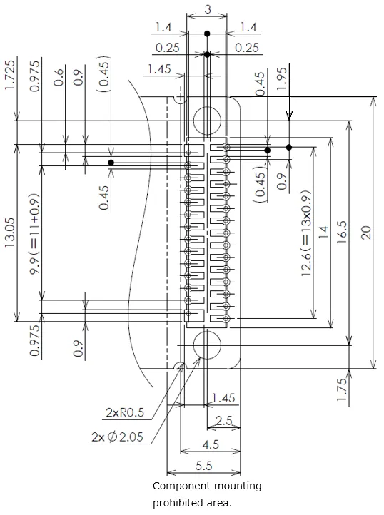
For board layout data, see AX02 29pin. Board design templates are available under Custom Leaf Development.
Names and Roles of the 29 Contacts
Section titled “Names and Roles of the 29 Contacts”The table below lists the common contact names shown in the AP01 and AP03 pin assignment diagrams. Numeric signal names in those diagrams, such as 8, are written as D8 here. Distinguish contact numbers such as F1, bus signal names such as D8, and MCU port names such as PA9.
| Contact number | Bus signal name | Role and checks |
|---|---|---|
| 1 | 3V3 / 3.3V | 3.3V power line. Check which leaf supplies or receives power and the current required |
| 2 | Res1 | MCU-specific function; SWDIO on AP03 |
| 3 | VBUS | Line associated with USB power. Check its connection and use on each leaf |
| 4 | AREF | Analog reference voltage connection; may be unconnected |
| 5 | RESET | Reset signal |
| 6 | A0 | Analog input or other function. Check the MCU assignment |
| 7 | D6 | Digital I/O or peripheral function |
| 8 | A1 | Analog input or other function |
| 9 | D7 | Digital I/O or peripheral function |
| 10 | A2 | Analog input or other function |
| 11 | D8 | Digital I/O or peripheral function |
| 12 | A3 | Analog input or other function |
| 13 | D9 | Digital I/O or peripheral function |
| 14 | A4 | Analog input or other function |
| 15 | D10 | Digital I/O or peripheral function |
| 16 | A5 | Analog input or other function |
| 17 | D11 | Digital I/O or peripheral function |
| 18 | D0 | Digital I/O or peripheral function |
| 19 | D12 | Digital I/O or peripheral function |
| 20 | D1 | Digital I/O or peripheral function |
| 21 | D13 | Digital I/O or peripheral function |
| 22 | D2 | Digital I/O or peripheral function |
| 23 | SDA | I2C data |
| 24 | D3 | Digital I/O or peripheral function |
| 25 | SCL | I2C clock |
| 26 | D4 | Digital I/O or peripheral function |
| 27 | GND | Power and signal reference |
| 28 | D5 | Digital I/O or peripheral function |
| 29 | Res2 | MCU-specific function; SWCLK on AP03 |
Check each leaf’s pin assignment diagram for contact positions and front/back orientation. This table does not specify absolute maximum electrical ratings or the internal connections of every leaf.
Functions That Depend on the MCU
Section titled “Functions That Depend on the MCU”The MCU port, UART/SPI/PWM functions, and Arduino pin number associated with a bus signal can differ between boards. Check the selected board definition against the pin assignments in your example.
For example, the AP03 pin assignment diagram connects D8 to PA9 and D9 to PA10 for UART use. On AP03B, a switch between D9 and PA10 disconnects them when BOOT0 is High. AP03B’s AREF is also unconnected to the MCU in its standard assembly. Matching contact names do not mean that swapping a leaf preserves the same behavior.
Checking Power and Signals
Section titled “Checking Power and Signals”- Distinguish 3.3V from VBUS. Check the power supplied by the USB leaf and battery leaf, and the power received by each connected leaf. Do not treat a power input voltage range as the allowable voltage for GPIO (general-purpose input/output) pins.
- Check multiple power sources. Before connecting USB and a battery together, check reverse-current protection and simultaneous supply conditions for each power leaf. AZ01C USB-C explains its different power states.
- Compare shared signal assignments. Check inputs, outputs, UART/SPI pins, reset signals, and interrupt connections on each leaf. Whether multiple outputs can share a line depends on their circuits and control methods.
- Check I2C addresses and pull-ups. Use the I2C Address Map to compare devices sharing SDA/SCL. Check the pull-up resistors on each MCU and sensor leaf.
Related Guides
Section titled “Related Guides”- Combining Leaves and Choosing a Power Supply: checks before selecting a configuration
- Assembling and Replacing Leaves: connectors, spacers, and fastening parts
- Pin Assignment Editor: compare pin usage across leaves
- Custom Leaf Development: CAD templates and design documents